Playing with the Pico Part 5 - Producing VGA Video
Lets talk about VGA signalling. VGA uses 5 wires, 3 are analog signals and represent red, green and blue, the higher the voltage the brighter the colour. The other 2 are sync and are digital signals, they tell the monitor how the colour signals relate to the pixels.
One of the sync signals is the horizontal sync (HSYNC), the other is the vertical (VSYNC). They both work in very similar ways, let’s take a look at the horizontal sync first. Below is a timing diagram that illustrates a single horizontal line of video, known as a scanline.
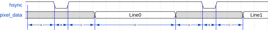
The HSYNC is just a pulse between scanlines. It is ordinarily held high and goes low for the sync pulse. The critical thing is the timing, driven by the pixel clock. The pixel clock measures how quickly the RGB signals change, each tick of the pixel clock means a new RGB value and a new pixel. The timing of the sync pulse is measured in terms of the pixel clock. Along with the sync pulse we have the back porch and the front porch, no pixels are output during all three. This is known as the horizontal blanking period. On CRT monitors this was required to allow the beam time to get back to the left side of the screen. I’ve marked the front and back porch and sync pulse along with the visible line on the diagram with letters. Here’s the length of each in pixel clocks at 640x480:
- A - front porch - 16 pixel clocks
- B - sync pulse - 96 pixel clocks
- C - back porch - 48 pixel clocks
- D - visible line - 640 pixel clocks
The VSYNC does exactly the same thing, only the timing is done in scanlines. Again there are front and back porches around the sync pulse and a visible region. This means again there’s a point where nothing is displayed known as the vertical blanking interval. This is used by CRT monitors to give time for the beam to go back to the top of the screen. Here’s a timing diagram showing horizontal and vertical sync.
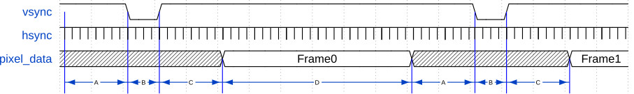
- A - front porch - 10 scan lines
- B - sync pulse - 2 scan lines
- C - back porch - 33 scan lines
- D - visible lines - 480 scan lines
The PIO program described in the last blog will be the basis of a PIO program to produce the horizontal and vertical sync signals. For each line (both those in the visible portion and the blanking portion) we’ll have 4 command words, one for each of the sync pulse, back and front porch and the visible portion. The delay part of the command word gives the delay and the pin settings control the vertical and horizontal sync outputs.
The program requires one extra feature, a way to signal when we are at various parts of the line or frame. In particular we want something to sync up another PIO program, one that will output our pixel data, with the beginning of a visible line.
We’ll use a special destination of the out instruction to do this. out can
write to an exec destination. What this does is shift data from the OSR and
immediately execute it as a PIO instruction. This will be used to add a PIO
instruction to the command word. The sync PIO program will sit in a loop,
pulling a 32-bit command word from the TX FIFO doing three things:
- Set HSYNC and VSYNC based on the bits 0 and 1
- Execute the PIO instruction from the command (bits 17 - 2)
- Enter a delay loop, delaying the number of cycles from the command (bits 31 - 18)
This is just my previous test program with the addition of the instruction
execution at 2. The instruction will either be nop doing nothing or irq
raising an interrupt that will signal the beginning of a line. To produce a full
frame of sync we just need to send the correct command words to the sync SM.
Here’s the PIO code:
.program sync_out
    pull ; get next command word
    out pins, 2 ; first 2 bits are hsync/vsync
    out x, 14 ; next 14 bits are delay
    out exec, 16 ; final 16 bits are instruction to execute
wait_loop:
    jmp x--, wait_loop ; wait for the given delay value
.wrap
To go along with this we need something to produce the pixel data. We’ll use a separate SM I’ll call the line SM that just pulls pixel data out of a FIFO and writes it out to the pins. We’ll use a 15-bit format of 5 bits red, 5 bits green and 5 bits blue with an external digital to analog converter (DAC) to produce the varying voltages for the VGA signal (16 bit with an extra bit for green is more usual but I only implemented 5 bits per channel on my DAC).
The line SM will sync itself up with the sync SM using the wait instruction to
wait for a start of line IRQ from the appropriate sync SM command word. When the
wait is done it will stream the pixel data from the FIFO out to the pins.
Initially I’m going to use the logic analyzer setup from the last blog to test
things (no monitor connected to the pins) so to keep it simple we’ll have 10
pixels per line and only 6 bits per pixel (giving 1 byte per logic analyzer
sample, 6 bits of pixel and 2 bits of sync). Here’s the line PIO program:
.program line_out
    wait 1 irq  4 ; wait til triggered by sync SM
    set x, 9 ; Setup x as pixel counter (10 pixels in a line)
line_loop:
    pull ; get next pixel
    out pins, 6 [7] ; output to the pins and delay (to give 10 cycles per loop)
    jmp x--, line_loop ; output next pixel if we have pixels left
end:
    set x, 0 ; output a 0 pixel after the visible line
    mov pins, x
.wrap
The pixel data needs to change at the pixel clock rate. For 640x480 that is 25.175 MHz. You can get away with not being too precise so the pixel clock will be 25 MHz, a nice multiple away from the Pico’s default 125 MHz (one pixel per 5 cycles). I’m actually going to produce graphics at 320x240 just to minimise the number of pixels to produce per frame but do this by outputting the same pixel twice in each line rather than producing a native 320x240 video signal. Overall this means the line PIO needs to output a new pixel value once every 10 cycles.
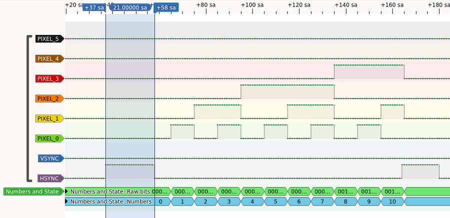
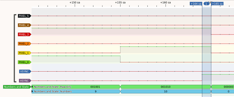
Here’s the command words we’re feeding the sync PIO program, delays don’t yet
correspond to actual VGA timings, we’re just using a few low numbers to see what
it produces. The VSYNC line is kept low and the HSYNC line switches with each
new command word, rather than producing proper sync pulses. This will allow us
to analyse how the delays relate to our output. We’ll look at everything in
reference to when the out pins, 2 instruction executes on the sync SM (I’ll
refer to it as the sync pin set). By switching the HSYNC line every new command
word the positive and negative edges of the HSYNC line show us when the out pins, 2 instruction is being executed.
|
|
For the pixel data we’ll just use numbers 1-40. The line PIO outputs 0 when we’re outside of the visible region so 1-40 is used so we can see when we’re in the pixel output loop part of the line PIO. Here’s the result showing the first line:
Full code can be found on github
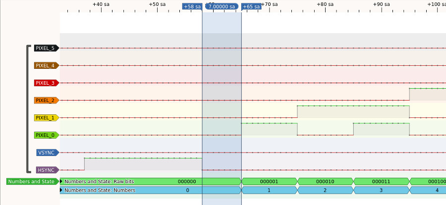
How does the delay value in the command word map to the cycles seen for each
low/high period of the HSYNC? The sync PIO program has 5 instructions so with a
delay of 0 you’d expect the HSYNC to be held high or low for 5 cycles. But it’s
actually 6. The out exec, 16 is hiding an extra cycle, one cycle to shift an
instruction from the OSR, another cycle to execute it. If we measure the high
and low periods of the HSYNC line we find they each take the corresponding delay
value + 6 as expected. E.g. look at the bit highlighted in blue where HSYNC is
held high. This corresponds to sync_timing_buffer[2], that has a delay value
of 15 and HSYNC is held high for 21 cycles (15 + 6).
The trickier part is how the timing of the command words relates to the line SM
which outputs the pixel data. Look back at the sync program. After fetching a
new command word it immediate sets the pins, reads the delay value and executes
an instruction via out exec and delays after all of this is done. The irq
instruction is used to trigger the pixel output from the line SM. The line SM
will execute its set x, 9 instruction two cycles after the irq instruction
is executed. One cycle after the irq is executed the wait 1 irq 4
instruction sees it’s been raised, so the cycle after than set x, 9 is
executed. The two PIO programs line up like this:
|      Sync SM                        |                       Line SM                                     |
-----------------------------------------------------------------------------------------------------------
| out pins, 2                         | wait 1 irq  4 ; line SM waiting for irq 4                         |
| out x, 14                           | wait 1 irq  4                                                     |
| out exec, 16                        | wait 1 irq  4                                                     |
| [irq 4]      ;irq from command word | wait 1 irq  4                                                     |
| jmp x--, wait_loop                  | wait 1 irq  4 ; irq 4 set last cycle, so final cycle of wait here |
| jmp x--, wait_loop                  | set x, 9                                                          |
| jmp x--, wait_loop                  | pull                                                              |
| jmp x--, wait_loop                  | out pins, 6 [7]                                                   |
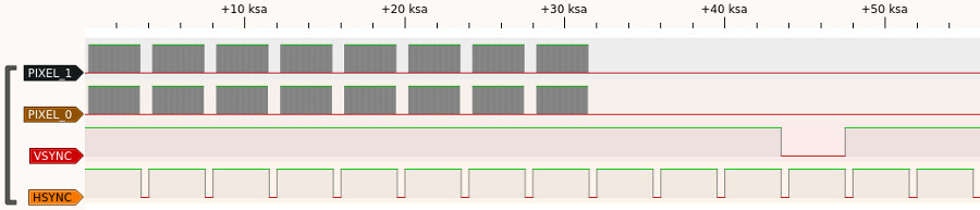
Looking at this you can see there’s 7 instructions between pins being set in the sync SM based on the command word and the first pixel being output in the line SM. This results in a delay of 7 cycles between the two. We can measure the gap on the logic analyzer output to confirm:
How about at the end of the line? What delay do we need in the sync SM command word for the visible part of the line so that the pin set of the next sync SM command word lines up with 0 pixel output at the end of the line? The Line SM outputs a new pixel every 10 cycles, so the time taken from the first pixel output to the 0 pixel output is 100 cycles. In total we have 107 cycles between the sync SM setting the pins and the 0 pixel output. Between pin settings in the sync SM we have 6 cycles + the delay value. To get the pin set to match with the 0 pixel output we want a total of 107 cycles between pin settings giving us a delay value of 101 (107 = 6 + 101). Our test command words used a delay value of 100 for the visible line, 1 less than we need. If we look at the logic analyzer the pin setting for the front porch command word happens 1 cycle before we see the 0 pixel, confirming our analysis.
Finally before we can produce a proper video signal we need to tweak our line
PIO program. It sets x to 9 as a pixel counter, we’ll have 320 pixels each
line and set only has 5-bits of immediate (so 31 is the biggest value we could
set x to). We work around this using the input shift register to make 319 out
of individual 5-bit pieces, we’ll also want to output 16 bits per pixel (the top
bit gets ignored but then a pixel is 2 bytes making the image encoding simpler).
.program line_out
    wait 1 irq  4 ; wait til triggered by sync SM
    set x, 31 ; Setup x as a pixel counter (x = 319)
    in x, 5
    set x, 9
    in x, 27
    mov x, isr
line_loop:
    pull ifempty ; only pull if we've shifted out two pixels (32 bits)
    out pins, 16 [7] ; output to the pins and delay (to give 10 cycles per loop)
    jmp x--, line_loop ; output next pixel if we have pixels left
end:
    set x, 0 ; output a 0 pixel after the visible line
    mov pins, x
.wrap
The new pixel counter setup adds some extra delay between the sync SM pin set and the first pixel output. It’s 4 extra instructions so that delay goes from 7 to 11 cycles.
With that analysis done we can work out the actual delays we need for proper VGA 640 * 480 timings. Remember our pixel clock is 25 MHz and the pico is running at 125 MHz so the VGA timing values above need multiplying by 5. Here’s the final delays we’ll use
- hsync pulse - 96 pixel clocks * 5 = 480 cycles, 480 - 6 = 474 delay
- back porch - 48 pixel clocks * 5 = 240 cycles, 240 - 6 - 11 (pixel output delay) = 223 delay
- visible line - 640 pixel clocks * 5 = 3200 cycles, 3200 - 6 + 11 (pixel output delay) = 3205 delay
- front porch - 16 pixel clocks * 5 = 80 cycles, 80 - 6 = 74 delay
Note the pixel output delay applied to the back porch and visible line timings. The back porch command delays for fewer cycles than the actual back porch as there’s 11 cycles between the visible line doing its sync pin set and the first pixel appearing and the actual back porch must be timed to end with the first pixel appearing. Similarly the visible line gains those cycles so the front porch sync pin set lines up with the 0 pixel being output. Luckily as the HSYNC and VSYNC don’t actually have to change between the back porch, visible line and front porch the timing different between the sync pin set happening and the pixel output doesn’t matter. Here’s our final set of command words to give horizontal sync timing for the visible line.
|
|
Next up is producing a full frame’s worth of sync. Luckily getting the horizontal sync and pixel output was the hard part. Vertical sync is timed in terms of lines so all we have to do is feed the same commands words we have for the visible line buffer with some slight tweaks. Producing the vsync pulse in the appropriate lines and only signalling the interrupt that starts line output in the visible lines. This gives us two extra command buffers:
|
|
There’s just one ‘vblank porch’ buffer for both front and back porch as they’re identical in terms of what happens each line.
To tie this all together we’ll use two DMA channels, one will feed the sync SM with command words and the other will feed the line SM with pixel data. We can use a DMA transfer complete interrupt handler to coordinate it all. For both we need to keep track of what line is next for each SM, noting it may not always be the same. The sync SM FIFO can hold 8 command words, 2 lines worth which the sync DMA will swiftly fill. Meanwhile we have 320 pixels, 160 32-bit words, for the line DMA to transfer. Thus the sync DMA channel can be a couple of lines a head of the line DMA channel. Here’s the interrupt handler:
|
|
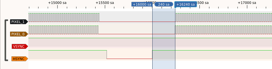
At this point it’d be great if we had sufficient memory to capture a full frame’s worth of pixel output and sync with the logic analyzer SM but we don’t. Instead to test things I temporarily dropped to 2 bits per pixel, maintained the same horizontal line timings but only output a small number of vertical lines, 8 visible lines, 1 VSYNC line, 3 front porch lines and 2 back proch lines. For the 2-bit pixel data I used an alternating 01, 10 pattern. This lets you see the pixels change as well as providing distinct visible and blank portions on the pixel data (only time we should see 00 is when we’re not outputting pixel data). With this restricted frame we can fit everything in memory, here’s the result from the logic analyzer:
I zoomed around on this, measuring the various intervals, for example here’s a zoom of the beginning of a line measuring the back porch (the time between the sync pulse and the beginning of the visible line). It is 240 cycles long, so 240 / 5 = 48 pixel clocks, exactly the timing we need. I checked all of the timings and everything looked good. We are ready to produce video!
Well almost, how exactly are we generating the pixels to show? The observant
will note the interrupt handler just has a buffer for a single line
line_data_buffer, there is no frame buffer. This is for memory reasons. The
Pico does just have enough memory for a 320x240 framebuffer at 16 bits per pixel
(320 * 240 * 2 = 150 KiB) but I plan to generate pixel data on the fly rather
than using a framebuffer. I’ll get into the details in the next blog, for now
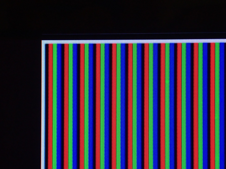
we’ll make do with a test pattern, one pixel of red, one of blue, one of green
and one of black repeated over and over. I’ll put a white pixel at the beginning
and end as well as make a modification to the interrupt handler to use a
different buffer of entirely white pixels for the first and last lines. This
will give a white border to the test pattern and allow us to check the edges of
the screen end up being where we think they are. Here’s the modified part of the
interrupt handler:
|
|
Full code can be found on github
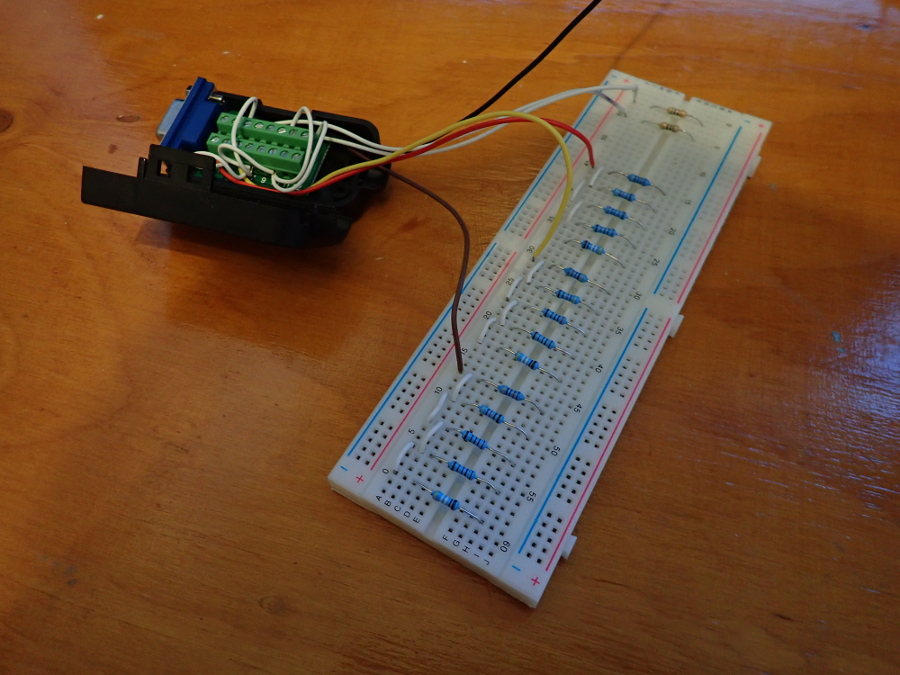
Finally how do we actually connect the VGA cable up to the pico? One answer is the Pimironi Pico VGA Demo Base which I haven’t yet bought (indeed it wasn’t available when I started working on this) but it’s easy enough to rig it up yourself. The sync lines can connect straight through via current limiting resistor. For the R,G,B lines you can create a primitive but effective digital to analog convertor using just some resistors, see Hardware design with RP2040 for the gory details (Chapter 3 which describes a board very similar to the Pimoroni one). Here’s a photo of my breadboard setup wired into a VGA connector breakout (which you can obtain from ebay or amazon).
With everything now in place let’s connect up the monitor, run our test program and see what happens…
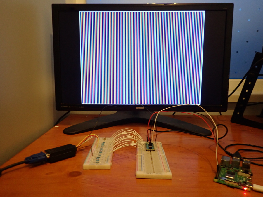
Success! Here’s a screen close up so you can see the pattern better:
Note that it’s important not to setup or try to use the USB UART (don’t call
stdio_init_all, printf etc). It seems to interfere with the video signal
generation and cause some visual artifacts, probably because of interrupts
dealing with USB. The plain serial UART may work fine but I haven’t tried it
out.
Next up we want to produce something more interesting than a test pattern which I’ll discuss in the next blog.