Playing with the Pico Part 4 - Getting Acquainted with PIO
I wanted to learn more about the RP2040’s PIO (programmable input/output) functionality. The PIO is a unique feature of the RP2040 which gives you fast precise control of the GPIO pins with programmable state machines. On other microcontrollers where you need to implement an interface (such as I2C or SPI) where hardware support isn’t available or you want more interfaces than the hardware provides you need to ‘bitbang’. Writing a program that manually toggles and reads pins, sometimes requiring careful programming to time things correctly. PIO can do this instead freeing the CPU cores to do other things.
PIO is very powerful once you get to grips with it. One thing it can do is generate video signals which I decided to try implementing myself. One impressive example runs dual DVI displays directly off an RP2040 with a suitable PCB. I was aiming for something simpler, VGA. Full code to produce VGA is available in the pico-extras repository in the pico_scanvideo library but I was interested in doing it myself from scratch (though I did take some ideas from scanvideo).
I used the C/C++ SDK Documentation and the RP2040 datasheet to learn about PIO. I’d recommend reading the SDK PIO guide first for a good introduction, the datasheet can then fill in the details. I’ll give a brief overview here.
PIO Introduction
There are two PIO blocks in the RP2040, each consists of 4 state machines (SMs) and a 32 word instruction memory. Each state machine (SM) has four registers, X & Y, and the input and output shift registers (ISR and OSR) which are all 32-bits in size. There are two FIFOs one for incoming data, the other for outgoing. The SM machine can control all 30 GPIOs, setting pin direction and output or reading input.
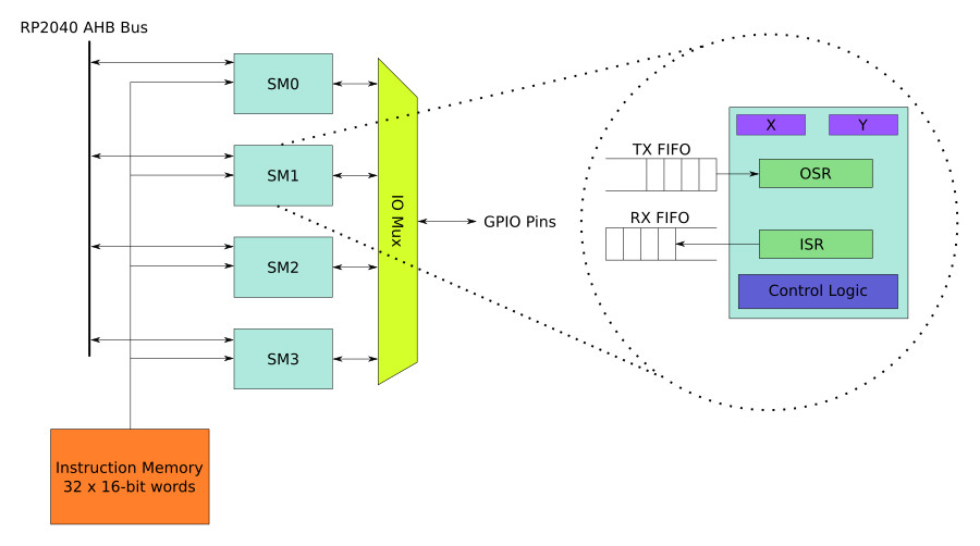
Instructions are 16-bit and there are 9 types:
- OUT- shift bits from the OSR into a destination, such as pin outputs or the X or Y scratch registers.
- IN - The opposite of OUT, shifting from sources such as pin inputs or the X or Y scratch registers into the ISR.
- PULL - pops the front element of the output FIFO into the OSR. Waits if the output FIFO is empty.
- PUSH - pushes the contents of the ISR into the input FIFO and clears the ISR. Waits if the input FIFO is full.
- MOV - Moves from a source to a destination. Can use registers and pins as both a source and destination as well as a couple of places with special functionality.
- JMP - Branches to a different instruction, can be conditional on a few conditions (such as X or Y zero or not-zero) and decrement X or Y.
- IRQ - Raises an interrupt (which can interrupt one of the cores or be used to synchronize SMs).
- WAIT - Can wait for various things like a pin changing state or an interrupt occurring.
- SET - Writes an immediate value to X, Y or the pins
Each instruction can have an optional delay measured in cycles which helps when you need precise timing and/or synchronization. There’s also something called ‘sideset’, this allows any instruction to additionally set pins in combination with whatever the instruction does. This is useful for control signals such as clocks and enables, the sideset deals with the control leaving the OUT, MOV or SET to just deal with data.
Here’s a simple example, it’s a PIO program that reads a byte from the output FIFO and outputs a bit a time (bits B0 - B7, LSB first) on a serial interface, generating a clock to go along with it, the data changes on the negative edge of the clock. It uses OUT to control the data pin and side set to control the clock pin.
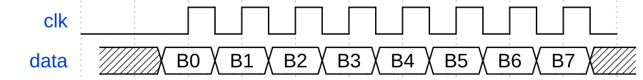
.program serial
.side_set 1 ; Tell the assembler we have one sideset pin

  pull     side 0 ; Read data from the output FIFO to the OSR, SM waits if there's none available
  set x, 7 side 0 ; Set up X as a bit counter. The PIO will loop outputting a bit each
                  ; time until the counter reaches 0
inner_loop:
  out pins, 1 side 0         ; Output one bit of the data shifting it from the OSR to the pins
  jmp x--, inner_loop side 1 ; Repeat the inner loop if X isn't 0 and decrement X (after checking
                             ; for zero).
  set pins, 0 side 0 ; Bring data low line at end of byte
.wrap ; Loop execution back to the beginning
The side 0 and side 1 controls the clock. Outside of the inner loop it
sidesets to 0, keeping the clock low. In the inner loop it toggles between 0 and
1 giving us positive and negative clock edges as the data shifts out bit by bit.
Like other hardware peripherals PIO provides a DMA DREQ. This means we can instruct the DMA to stream data to the PIO at the rate it’s being consumed. This allows what would otherwise be long and/or complex bit bang sequences to be performed entirely without CPU involvement.
There’s plenty more functionality I don’t describe above, read the documentation to find out more.
First steps with the PIO
I started by playing with the blink example just to check I’d got the basics correct. Blink reads a number from the output FIFO which it uses as a delay. It turns a pin on for that number of cycles then turns it off again for the same number of cycles. Here’s the PIO code:
.program blink
    pull block
    out y, 32
.wrap_target
    mov x, y
    set pins, 1   ; Turn LED on
lp1:
    jmp x-- lp1   ; Delay for (x + 1) cycles, x is a 32 bit number
    mov x, y
    set pins, 0   ; Turn LED off
lp2:
    jmp x-- lp2   ; Delay for the same number of cycles again
.wrap             ; Blink forever!
I tweaked this so it would keep reading from the PIO TX FIFO to get new blink counts every time and fed this with a DMA channel.
.program blink
.wrap_target
    pull block
    out y, 32
    mov x, y
    set pins, 1   ; Turn LED on
lp1:
    jmp x-- lp1   ; Delay for (x + 1) cycles, x is a 32 bit number
    mov x, y
    set pins, 0   ; Turn LED off
lp2:
    jmp x-- lp2   ; Delay for the same number of cycles again
.wrap             ; Blink forever!
In doing so I found it’s very important to start a DMA channel that transfers to a PIO FIFO after the relevant state machine has been initialised and not before. If you do it before the DMA never seems to transfer anything and the PIO hangs forever waiting for data.
Next I started putting together what I needed to generate a VGA signal. I wanted a PIO program that would toggle two bits with timings supplied via the FIFO (I’ll explain the point of this in the next blog where I go over VGA signalling). I wrote the following PIO program which pulls a 32-bit word from the FIFO, uses the lower 2 bits to set two pins then the upper 30 bits for a delay value.
Full code can be found on github
.program pin_ctrl
    pull block  ; Grab next command word
    out pins, 2 ; Bottom 2 bits are next pin setting
    out x, 30   ; Other 30 bits give a delay
wait_loop:
    jmp x--, wait_loop ; Delay for (x + 1) cycles
.wrap
Here’s the data we’re feeding the PIO:
|
|
The pico-examples repository contains a ‘logic analyser’ which just reads pin state and pushes it to a FIFO which DMA streams into a capture buffer. This gives you a buffer with regular samples of whichever in pins you configure for the SM the logic analyser is running on. Combined with a wait that holds the analyser SM until a particular pin becomes true or false as a trigger you have a very primitive logic analyser. I connected this up to my example, with one modification, I had it dump the capture buffer in a .csv format suitable for loading into PulseView, an open source logic analyzer software package.
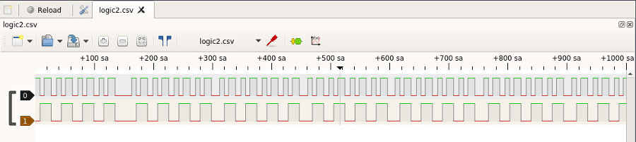
Here’s the pattern seen by the logic analyzer:
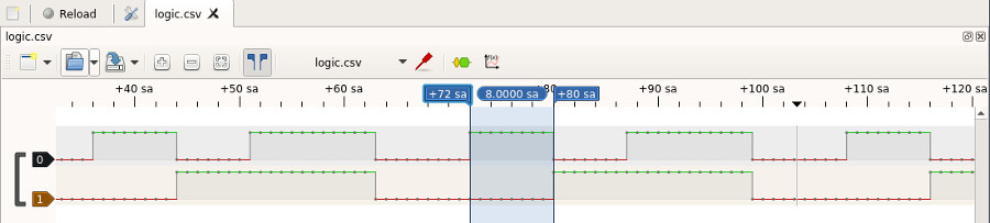
The two bits were behaving as expected, the highlighted section is the first
line from the timing_buffer. The 0x1 outputs 1 on the first pin and 0 on the
second pin and there is a delay of 4. There are 4 instructions in the loop
and each instruction takes 1 cycle so there is a minimum of 4 cycles per loop
giving a total of 8 cycles which is the time our trace shows the 0x1 setting
being held for. Each step of the pattern has the expected timings and it all
loops nicely.
Running PIO SMs without stalling
The one thing to beware of is the speed of the PIO. It will take 40 cycles for it to go through the entire timing buffer (4 + 3 + 8 + 5 delays + 4 * 4 for the fixed overhead). We’ll need to be handling a DMA interrupt starting a new transfer once every 40 cycles on average to keep things going and avoid stalling the SM. Probably more than we can manage (plus the CPU will spend all its time in DMA interrupts). We can get around this using a ring buffer. The DMA can be set to wrap the read address on power of two sizes. The timing buffer is 16 bytes so if we set the DMA to wrap and give it a multiple of 4 transfers to do it’ll feed the PIO with the timing buffer multiple times before a interrupt needs to restart things. Here’s the code that performs the DMA setup:
|
|
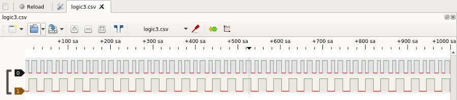
There’s still a problem though, let’s zoom out in the capture above (where the ring buffer was used):
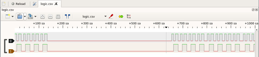
We get a few repeats of the pattern and a long gap where the SM is stalled. The
long gap is caused by the flash cache on the pico. The interrupt handler code is
off chip initially so there’s a long delay when it’s first fetched and executed
leading to a long pause in our PIO output whilst it waits for the DMA to start
again. We can try and fix this by using __not_in_flash_func with our interrupt
handler so it gets placed into SRAM.
|
|
Looking better but there’s still the occasional gap that’s longer than it should be. Ultimately what we’re trying to do is here is quite demanding, once the DMA has finished there’s not much time til the PIO SM has drained its TX FIFO and the DMA has to have started again. The TX FIFO is only 4 entries but if we’re not using the RX FIFO we can double the size of the TX FIFO to 8. By using that doubling here we can remove the gaps entirely
|
|
So how does this relate to video signals? I’ll go into that in the next blog.